SHIFT is a European Commission (EC) funded Integrated Project in the
frame of the IST (Information Society Technologies) Programme (contract
number 507745), selected from the call FP6/2002/IST/1 under the priority 2.3.1.2 "Micro and Nano Systems" Some key figures :
Starting date : January 1, 2004
Finishing date : December 31, 2008
Duration : 4 years
Total budget (approx.) : 11.5 MEuro
Funding (EC + Swiss) : 5.85 MEuro
8 participating partners from 5 different EC member/associated
countries (Belgium, Germany, France, Switzerland, Finland); additional partner(s) to join later on in the project
70 person-years of effort to be spent on the project
1. Project summary
The objective of the project is the development of smart, high-integration,
mechanically flexible electronic systems, for a wide variety of applications. “Smart” means that the flexible multilayer
laminate has embedded components, and that the different flex layers in the multilayer structure can have different functions,
meaning that it might be necessary to combine layers of different base material in the laminate. Compactness of the resulting
circuit will be boosted in two ways : by using the third dimension for electronic component integration (not only on front and
back side, but potentially on every conductive layer) and by drastically increasing the wiring density through the
introduction of new flex manufacturing and lamination techniques. Innovative technologies to be developed in SHIFT include
a new, cheap flex laminate technology, based on a process for
electroless Cu deposition on polyimide
a new lamination technology, based on interconnection by solid
state diffusion
The rationale of the project is that in order to realise the "ambient
intelligence" vision, more and more electronics systems will accompany the citizen. For these systems there is a trend towards
increased functionality, compactness, wearability and reduced weight. The system may not hamper the mobility of the human
carrier. Flexible electronics systems take the shape of the object onto or into which they are placed and may become quasi
non-noticeable to the user. Compared to their rigid board counterparts they show a drastic increase of comfort for the user,
and therefore the trend is starting and will become only stronger towards the use of "smart" comfortable mechanically flexible
electronic systems. The aim of SHIFT is precisely to develop enabling technologies for such complex flexible electronic
systems.
2. Project objective(s)
The SHIFT vision
In order to realize the “ambient intelligence” vision it is clear that more
and more electronics systems will accompany the citizen. These electronics systems, moving along with the owner, and present
near the body (e.g. portable communication systems), on the body (e.g. smart textiles), or even inside the body (implants),
will have to communicate with each other and with systems, which are fixed in the ambient. It is clear that the “carry-along”
electronic systems may not hamper the comfort of the human “carrier” too much, even must almost be non-noticeable to the user.
Therefore they must be lightweight and compact, must preferably take the shape of the object in which they are integrated,
must be highly functional at a reasonable price. For this reason the logic evolution will be such that present rigid
electronic substrates and assemblies will be replaced by flexible counterparts. This trend is just starting and will become
stronger in the coming years. To boost the combination of high functionality and compactness / comfort, there is a strong need
for substantial technology developments on flex technologies. This is exactly what SHIFT will aim to do.
State of the art
Flexible materials are being used already today as base substrates for
electronic assembly. Typical materials include polyimides for high-end applications down to cheap paper-like or plastic
materials like PET for very cost-sensitive applications. In this project we will concentrate on this “high-end” type flex
substrate materials like polyimide, LCP (liquid crystal polymer) etc. Manufacturers of these types of flex circuits detect an
increasing interest in a wide variety of fields for flex technology.
The
development of high density and high performance flexes is mainly driven by applications as LCD, HDD, DVD and consumer
products as camcorders or foldable mobile phones. The needs for the interconnection of LCDs, especially color LCDs and the
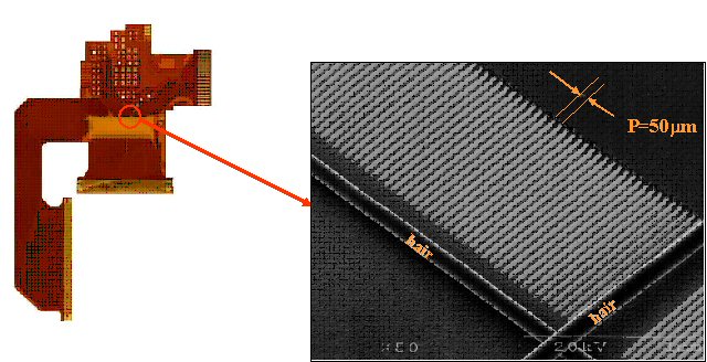
increasing demands on the resolution are pushing the limits of the technology for single and double sided flexes. High volume
production reaches a pitch of 50 µm for single sided and 70 µm for double sided flexes. An example of a LCD interconnection
flex with a pitch of 50 µm is given in the picture below. Multilayers are mainly required in high end consumer products as
camcorders and the leading edge of technology was used for the motherboard of the Playstation 2 which was a 10 layer flex
build up with a 6 layer core and two sequential build ups. All features known from rigid boards as surface via, via on pad or
staggered vias are possible. Only a very restricted number of manufacturers in the Far East can provide these technologies and
the European manufacturers are far behind the capabilities of the Far East located companies especially if high volume
production is required.
Although enjoying an increasing popularity current flex substrate and assembly technologies still
have serious restrictions :
Normally a flex substrate is a 3-layer
laminate where a Cu sheet (layer 1, thickness typically minimum 12µm) is laminated onto a polyimide carrier (layer 2) using an
adhesive (layer 3). Thinner Cu is not possible because of mechanical constraints (danger for breaking of the thin Cu layer
during the lamination process). Although widely used these 3-layer laminates have following limitations :
The conductor pitch is limited to minimum 40-50m, because the
underetching of the Cu during wet etching process is proportional (and about equal) to Cu thickness
The Cu thickness puts a lower limit to bending radius of the
substrate
The presence of an adhesive has negative influence on feasibility
and reliability of certain advanced assembly technologies, like e.g. adhesive flip-chip (melting of laminate
adhesive during flip-chip thermocompression step)
Only a limited number of sources for adhesives are available; which
increases the price for 3-layer laminates
Also 2-layer laminates are offered on the market, where the Cu is deposited
onto the polyimide without the use of adhesive. These laminates are expensive because of the complex production process. The
problem is the adhesion of the Cu (or any other metal) onto the polyimide surface. The adhesion strength of a metal onto a
polyimide is normally very low. What is currently done in production environment to produce 2-layer laminates with sufficient
adhesion strength, is first modifying the polyimide surface by e.g. plasma treatment, followed by a thin-film deposition
(sputtering) of Cu onto the modified (more reactive) polyimide, followed by further increasing the Cu thickness by
electrolytic plating. In this case thin Cu layers with very fine pitch capability are possible, but it is clear that the use
of vacuum processes (plasma treatment, sputtering) increases the price of the product considerably. Another production method
for 2-layer laminates, used in Japan, is the deposition of liquid polyimide layers onto Cu films followed by an imidization
process at high temperatures in a nitrogen atmosphere. This is a cheaper production process, but the restriction here is also
the minimum required Cu thickness for mechanical reasons, thus limiting the minimum achievable pitch. The lamination of two
single sided materials using a thermoplastic polyimide adhesive is used to get double sided materials. Today such 2-layer
laminates have a minimum Cu thickness of 12 µm
So a decrease of the
price of the base substrate is a vital issue for wider use of high-end flex, and especially cheap high-end flex base
substrates with very fine pitch capabilities (thin Cu conductor layers) do not exist today.
On this type of flex only pure electronic assembly is performed up to flip-chip components.
Embedding of passive or active components in flexible printed circuits is at least not state of the art and is, to the
knowledge of the consortium, not performed anywhere in the world so far, certainly not on a commercial basis. The limitation
to two component layers (front and back side of the flex laminate) limits the compactness of the circuit.
Objective
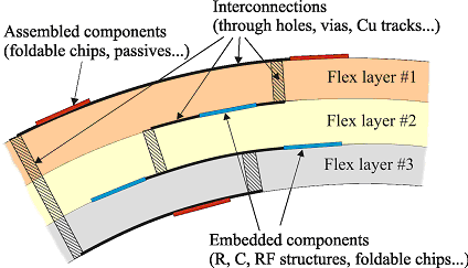
The objective of the project is the development of smart, high-integration,
mechanically flexible electronic systems, for a wide variety of applications. “Smart” means that the flexible multilayer
laminate has embedded components, and that the different flex layers in the multilayer structure can have different functions,
meaning that it might be necessary to combine layers of different base material in the laminate. The principle of such smart
flex, including assembled components, is shown in the figure below. Compactness of the resulting circuit will be boosted in
two ways :
By using the third dimension for electronic component integration
(not only on front and back side, but potentially on every conductive layer)
By drastically increasing the wiring density through the
introduction of new flex manufacturing and lamination techniques
In order to achieve the final goal of smart, compact flex assemblies a logical
build-up of activities is foreseen in the project :
Development of a number of generic base technologies :
New cheap high density flex base substrate manufacturing process
through electroless Cu deposition technology on polyimide (“eCuflex”); goal is to reach a conductor pitch of 20µm
Process for PTH (plated through holes) and via holes in
high-density flex, and for production of double-sided flex substrates
New multilayer flex lamination technology using solid state
diffusion technology, allowing to obtain highly reliable compact multilayer flex substrates
Extremely bendable multilayer high-density interconnection substrates (HiCoFlex)
with narrow pitch and small via holes, and its extension to Large Area Panels.
Development of technologies for embedding electronic components :
passives (R and C), RF structures, and ultrathin (20µm) foldable chips
Assembly (lead-free) of standard components and of ultrathin (20µm)
foldable chips with very small gap (10µm) onto flex laminates with embedded components, preserving mechanical
flexibility, even of a completely assembled circuit
Combination and integration of several functional layers, which may
be produced on different types of base substrate materials, e.g. the combination of a high density digital circuit
on a polyimide substrate, together with an RF circuit, produced on an LCP substrate, thus creating the possibility
for complex, high-functionality flex circuits.
Modelling and testing
The technological developments will be supported by modelling activities
(electrical, mechanical, thermal and thermal-mechanical) and testing (especially reliability testing) in order to qualify the
technologies, and facilitate design of multilayer, embedded flex circuitry. These supporting activities will be carried out
throughout the project.
Cost effective production processes
To make price competitive products not only the base materials should be cheap,
but high volume products should be manufactured in a cost effective way. Therefore during the development of base technologies
and flex integration processes the possibility to implement these technologies in a reel-to-reel production system should be
kept in mind. After feasibility demonstration actual development and implementation of the necessary reel-to-reel processes
for multilayer flex manufacturing, component embedding and assembly, is programmed. When reel-to-reel processing is not
possible for a developed technology, a second way for cost-effective manufacturing will investigated, namely large area
production (LAP).
Demonstration activities
During the second phase of the project the developed generic base flex
technologies and the integration of these technologies into smart flex systems will be demonstrated by designing and producing
functional prototypes/demonstrators.
From the first phase of the project
on (generic basic technologies development) the activities will be triggered by the end-users in the consortium.
It is strongly believed that for each degree of flex complexity, from ‘simple’
single-sided high density flex up to the most complex multilayer flex systems, potential applications can be found. In this
way, bringing together the right basic blocks of flex substrate production, component integration and assembly, the
technologies developed in the proposed SHIFT project, will lead to applications in a very wide variety of industrial sectors.
The proposed technological objectives are clearly beyond the current
state of the art world-wide : component embedding in flex does not exist today, proposed cheap, high density eCuflex flex
manufacturing and solid state diffusion lamination techniques are original, embedding and assembly of ultra-thin (20µm) chips
on embedded flex is an innovative technology, and so on. Successful developments in SHIFT will truly open up a vast number of
opportunities to come closer to the ambient intelligence vision.
3. The
partnership
To tackle the challenges of the project a founding consortium has been formed,
consisting of 3 R&D institutes, 2 industrial flex manufacturers, 2 large end-users and an engineering association for
financial and administrative management. Part of the budget is available for integration later on in the project of one or
more aditional partner(s). Priority will be given to an additional end-user. This additional partner will join the consortium
after 2 years (Jan.1, 2006). A competitive call will be launched mid 2005 for the selection of this additional end-user. The
selection will depend on the applicability and the potential of exploitation of the successfully developed SHIFT technologies
in the products of the additional end-user.
Participant name
Participant short name
Country
Type
Interuniversitair Micro-Elektronica Centrum vzw
IMEC
Belgium
R&D Institute
Technische Universität Berlin
TUB
Germany
R&D Institute
Fraunhofergesellscahft zur Förderung der angewandten
Forschung e.V.,
FhG
Germany
R&D Institute
Freudenberg Mektec Europa GmbH
Mektec
Germany
Industry : Flex manufacturer
Hightec MC AG
Hightec
Switzerland
Industry : Flex manufacturer
Nokia Research Center
NRC
Finland
Industry : end-user
Thales Systèmes Aeroportes
Thales
France
Industry : end-user
VDI/VDE- Technologiezentrum für Informationstechnik GmbH
VDI/VDE-IT
Germany
Industry : Engineering association
Additional partner(s)
Industry : end-user
...
4. Dissemination activities : set-up of forum of interested external parties
It is believed that the technologies developed in SHIFT will be usable in a
wide variety of applications, besides those actually present in the consortium now : biomedical, smart cards, automotive,
consumer are only a few examples of additional potential application fields. Next to potential end-users, also entities like
equipment manufacturers, assembly houses, raw materials manufacturers, etc. should be aware of the developments in SHIFT and
vice versa. Therefore the dissemination activities in SHIFT are considered to be of the highest importance. It is the
intention to create a forum of European entities interested in advanced flex technologies and the application of these
technologies in any kind of products.
Therefore interested parties are asked to register as a member to receive
further information in the form of mailings and newsletters. Within the first months of the project, the partners will collect
contact dates of interested European persons and institutions. Target groups are :
participants of similar EU funded projects
companies with special interest in SHIFT production technologies
companies with suitable applications of SHIFT technology based
components in their products
university faculties with complementary or intersecting research
subjects
In connection with general assemblies of the SHIFT consortium or at other
appropriate dates, a yearly conference/network training meeting on SHIFT technologies will be held. (Months 13, 25, 37) This
conference is aimed at a close European circle of research institutes and companies in order to train a selected group of
participants in the SHIFT project’s results. It shall also be one element of the identification of new SHIFT project members.
If you have interest in joining this SHIFT forum, please contact the general or
administrative co-ordinator (co-ordinates below)
5. Contact
For more information, contact the
general project co-ordinator :